Many sensors output a voltage waveform. Thus no signal conditioning circuitry is needed to perform the conversion to a voltage. However, dynamic range modification, impedance transformation, and bandwidth reduction may all be necessary in the signal conditioning system depending on the amplitude and bandwidth of the signal and the impedance of the sensor. The circuits discussed in this section and in subsequent sections are treated as building blocks of a human-computer input system. Their defining equations for their operation are given without proof. For a more detailed description of how they work, see Design with Operational Amplifiers and Analog Integrated Circuits, Franco 1988 or The Art of Electronics, Horowitz and Hill 1989. It is especially important to review the analysis of ideal op-amp circuits.
Inverting
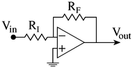
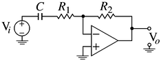
The most common circuit used for signal conditioning is the inverting amplifier circuit as
shown in Figure 15 This amplifier was first used when op-amps only had one input, the
inverting (-) input. The voltage gain of this amplifier is ![]() . Thus the level of
sensor outputs can be matched to the level necessary for the data acquisition system. The
input impedance is approximately
. Thus the level of
sensor outputs can be matched to the level necessary for the data acquisition system. The
input impedance is approximately ![]() and the output impedance is nearly zero. Thus,
this circuit provides impedance transformation between the sensor and the data acquisition
system.
and the output impedance is nearly zero. Thus,
this circuit provides impedance transformation between the sensor and the data acquisition
system.
Figure 15: Inverting Amplifier
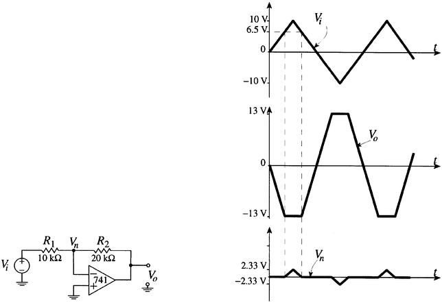
It is important to remember that the voltage swing of the output of the amplifier is limited by the amplifier's power supply as shown in Figure 16. In this example, the power supply is +/- 13V. When the amplifier output exceeds this level, the output is ``clipped''.
Figure 16: Clipping of an Amplifier's Output
Just as the dynamic range of the amplifier is limited, so too is the bandwidth. Op-amps
have a fixed gain-bandwidth product which is specified by the manufacturer. If , for
example, the op-amp is specified to have a ![]() gain-bandwidth product, and it is
connected to have a gain of 100, this means that the bandwidth of the amplifier will be
limited to
gain-bandwidth product, and it is
connected to have a gain of 100, this means that the bandwidth of the amplifier will be
limited to ![]() (
( ![]() ).
Another important limitation of the amplifier circuit is noise. All op-amps introduce noise
to the signal. The amount and characteristics of the noise are specified by the
manufacturer of the op-amp. Also, the resistors introduce noise. The equation for this
thermal noise is
).
Another important limitation of the amplifier circuit is noise. All op-amps introduce noise
to the signal. The amount and characteristics of the noise are specified by the
manufacturer of the op-amp. Also, the resistors introduce noise. The equation for this
thermal noise is ![]() ; where k is Boltzmann's constant, T is the
temperature, B is the bandwidth of the measurement device, and R is the value of the
resistance. The main point to remember, is the larger the resistor values used, the larger
the amount of noise introduced.
One more limitation of the op-amp is offset voltage. All op-amps have a small amount of
voltage present between the inverting and non-inverting terminals. This DC potential is
then amplified just as if it was part of the signal from the sensor.
There are many other limitations of the amplifier circuit that are important for the HCI
designer to be aware. Too many, in fact, to describe in detail here (refer to the previously
mentioned references.)
; where k is Boltzmann's constant, T is the
temperature, B is the bandwidth of the measurement device, and R is the value of the
resistance. The main point to remember, is the larger the resistor values used, the larger
the amount of noise introduced.
One more limitation of the op-amp is offset voltage. All op-amps have a small amount of
voltage present between the inverting and non-inverting terminals. This DC potential is
then amplified just as if it was part of the signal from the sensor.
There are many other limitations of the amplifier circuit that are important for the HCI
designer to be aware. Too many, in fact, to describe in detail here (refer to the previously
mentioned references.)
Non-Inverting
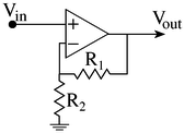
Another commonly used amplifier configuration is shown in Figure 17. The gain of this
circuit is given as ![]() . The input impedance is nearly infinite (limited
only by the op-amp's input impedance) and the output impedance is nearly zero. The
circuit is ideal for sensors that have a high source impedance and thus would be affected
by the current draw of the data acquisition system.
. The input impedance is nearly infinite (limited
only by the op-amp's input impedance) and the output impedance is nearly zero. The
circuit is ideal for sensors that have a high source impedance and thus would be affected
by the current draw of the data acquisition system.
Figure 17: Non-Inverting Amplifier
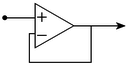
If ![]() and
and ![]() is open (removed), then the gain of the non-inverting amplifier is
unity. This circuit, as shown in Figure 18 is commonly referred to as a unity-gain buffer
or simply a buffer.
is open (removed), then the gain of the non-inverting amplifier is
unity. This circuit, as shown in Figure 18 is commonly referred to as a unity-gain buffer
or simply a buffer.
Figure 18: Unity-Gain Buffer
Summing and Subtracting
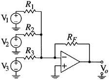
The op-amp can be used to add two or more signals together as shown in Figure 19.
Figure 19: The Summing Amplifier
The output of this circuit is ![]() . This circuit can be used to combine the outputs of many sensors
such as a microphone array.
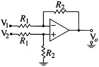
The op-amp can also be used to subtract two signals as shown in Figure 20 This circuit is
commonly used to remove unwanted DC offset. It can also be used to remove differences
in the ground potential of the sensor and the ground potential of the data acquisition
circuitry (so-called ground loops).
. This circuit can be used to combine the outputs of many sensors
such as a microphone array.
The op-amp can also be used to subtract two signals as shown in Figure 20 This circuit is
commonly used to remove unwanted DC offset. It can also be used to remove differences
in the ground potential of the sensor and the ground potential of the data acquisition
circuitry (so-called ground loops).
Figure 20: Difference Amplifier
The output of this circuit is given as ![]() . Thus
. Thus
![]() can be the output of the sensor and
can be the output of the sensor and ![]() can be the signal that is to be removed.
can be the signal that is to be removed.
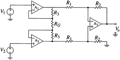
Instrumentation amplifier
Possibly the most important circuit configuration for amplifying sensor output is the instrumentation amplifier (IA). Franco defines the requirements for an IA as follows:
CMRR (common mode rejection ratio) is defined as:
![]()
Where:
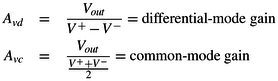
That is, CMRR is the ratio of the gain of the amplifier for differential-mode signals
(signals that are different between the two inputs) to the gain of the amplifier for
common-mode signals (signals that are the same at both inputs).
The difference amplifier described above, clearly does not satisfy the second requirement
of high input impedance. To solve this problem, a non-inverting amplifier is placed at each
one of the inputs to the difference amplifier as shown in Figure 21. Remember that a
non-inverting amplifier has a nearly infinite input impedance. Notice that instead of
grounding the resistors, the two resistors are connected together to create one common
resistor, ![]() . The overall differential gain of the circuit is:
. The overall differential gain of the circuit is:
![]()
Figure 21: Instrumentation Amplifier
Lowpass and highpass filters
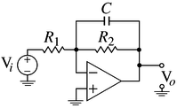
The non-inverting amplifier configuration can be modified to limit the bandwidth of the
incoming signal. For example, the feedback resistor can be replaced with a
resistor/capacitor combination as shown in Figure 22 Thus the gain of the circuit is now:
![]() where:
where:

Figure 22: Single Pole Low-Pass Filter
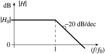
A filter ``rolls off'' at 20dB per 10-times increase in frequency (20dB/decade) times the
order of the filter, i.e.:
![]() .
Thus a first order filter ``rolls off'' at 20dB/decade as shown in Figure 23.
.
Thus a first order filter ``rolls off'' at 20dB/decade as shown in Figure 23.
Figure 23: Frequency Response of Single Pole Lowpass Filter
The input resistor of the inverting amplifier can also be replaced by a resistor/capacitor
pair to create a high pass filter as shown in Figure 24 The gain of this filter is given by:
![]() where:
where:

Figure 24: Single Pole High-Pass Filter
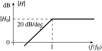
The frequency response of this filter is shown in Figure 25.
Figure 25: Frequency Response of a Single Pole High-Pass Filter
Higher order filters, which consequently have faster attenuation rates, can be created by cascading many first-order filters. Alternatively, the filter circuit can include more resistor/capacitor pairs to increase its order. The technique for doing this can be found in either of the references given previously. For the HCI designer, however, the two important steps are to determine the required filter order and to pick a circuit of that order - making sure that the circuit also meets any of the other previously described requirements of the signal conditioning circuitry.
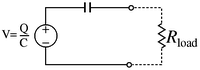
As mentioned previously, a common implementation practice is to sandwich a piezoelectric crystal between two metal plates. Figure 26 shows an equivalent electrical circuit of this arrangement. The voltage source represents the voltage that develops due to the excess surface charge on the crystal. The capacitor which appears in series is due to the capacitor formed by the metallic plates of the sensor. An important point to make is that piezo sensors cannot be used to measure a constant force, but rather is only useful for dynamic forces. If one is familiar with basic circuit theory, it should be clear that the capacitor blocks the direct current (the constant voltage resulting from a constant force).
Figure 26: A piezoelectric sensor with a load resistance
In order to measure the force, one must measure the voltage which appears across the
terminals of the sensor. It is impossible to measure voltage without drawing at least a
little electrical current. This situation is summed up in
Figure 26 where ![]() represents the load impedance inherent in the measuring
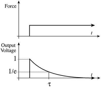
device. Figure 27 shows a typical response which might arise if a constant force is
applied to the piezo. In the absence of a load resistance, a force applied to the crystal will
develop a charge which will remain as long as the force is present. In the case where the
load resistor is present, an electrical path is formed which serves to allow the charge to
dissipate, which in turn reduces the voltage. The higher the value of the resistance, the
longer it will take for the charge to dissipate. The time-constant of the system is
defined as the time it takes the charge (or voltage) to decrease to approximately 37its original value. The time constant
represents the load impedance inherent in the measuring
device. Figure 27 shows a typical response which might arise if a constant force is
applied to the piezo. In the absence of a load resistance, a force applied to the crystal will
develop a charge which will remain as long as the force is present. In the case where the
load resistor is present, an electrical path is formed which serves to allow the charge to
dissipate, which in turn reduces the voltage. The higher the value of the resistance, the
longer it will take for the charge to dissipate. The time-constant of the system is
defined as the time it takes the charge (or voltage) to decrease to approximately 37its original value. The time constant ![]() is give by
is give by ![]() . Typical values for
common piezo sensors is about
. Typical values for
common piezo sensors is about ![]() ( nano-farads), and typical input impedances
for measuring devices is on the order of
( nano-farads), and typical input impedances
for measuring devices is on the order of ![]() ( mega-ohms). These values
result in a
( mega-ohms). These values
result in a ![]() of
of ![]() . Roughly speaking, this means that forces that are
constant, or vary slowely will suffer from the fact that the voltage across the sensor will
tend to decrease in amplitude, and the overall amplitude of the measure voltage will be
reduced. Alternatively, forces which vary rapidly will not be subject to much if any
decrease in amplitude.
. Roughly speaking, this means that forces that are
constant, or vary slowely will suffer from the fact that the voltage across the sensor will
tend to decrease in amplitude, and the overall amplitude of the measure voltage will be
reduced. Alternatively, forces which vary rapidly will not be subject to much if any
decrease in amplitude.
Figure 27: Time domain response of the output of a piezo sensor subject to a constant force
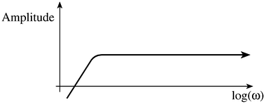
Figure 28: Frequency response of a piezo sensor
This situation can also be described in the frequency domain. In the time domain,
the system is characterized by its time constant whereas in the frequency domain it is
characterized by its cutoff frequency ![]() . A plot of the
frequency response of piezo sensor along with a load resistance is shown in Figure 28.
For the sensor mentioned earlier with an internal capacitance of
. A plot of the
frequency response of piezo sensor along with a load resistance is shown in Figure 28.
For the sensor mentioned earlier with an internal capacitance of ![]() and a
load resistance of
and a
load resistance of ![]() , the cutoff frequency is equal to
, the cutoff frequency is equal to ![]() .
Specifically, this means that a force varying at a frequency of
.
Specifically, this means that a force varying at a frequency of ![]() will result in a
measured voltage which is
will result in a
measured voltage which is ![]() less than a more rapidly varying force with the same
amplitude. In many applications it is important to make the
less than a more rapidly varying force with the same
amplitude. In many applications it is important to make the ![]() frequency as low as
possible. In order to do this one must make the input impedance of their measuring circuit
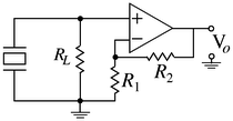
as high as possible. Thus a non-inverting amplifier is connected to the piezo output as
shown in Figure 29.
frequency as low as
possible. In order to do this one must make the input impedance of their measuring circuit
as high as possible. Thus a non-inverting amplifier is connected to the piezo output as
shown in Figure 29.
Figure 29: Amplified piezo sensor
Hence the circuit amplifies the voltage by the factor ![]() . The
. The ![]() cutoff frequency of this circuit is
cutoff frequency of this circuit is ![]() , where C is
the internal capacitance of the sensor. It is clear that an increase in the value of the input
resistor will result in a decrease in the cutoff frequency.
, where C is
the internal capacitance of the sensor. It is clear that an increase in the value of the input
resistor will result in a decrease in the cutoff frequency.
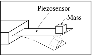
Figure 30: Using a piezoelectric sensor as an accelerometer
As mentioned several times, piezo sensors find many applications. Figure 30 shows a mechanical system which implements an accelerometer. In this system, a mass is placed on the tip of a piezo sensor forming a cantilever beam. When the mass undergoes an acceleration, a resultant force will cause the piezo film to bend, which will result in a voltage. Remember that the piezo sensor cannot measure a constant force, so this device can only measure dynamic acceleration, and cannot be used for applications such as tilt sensors.